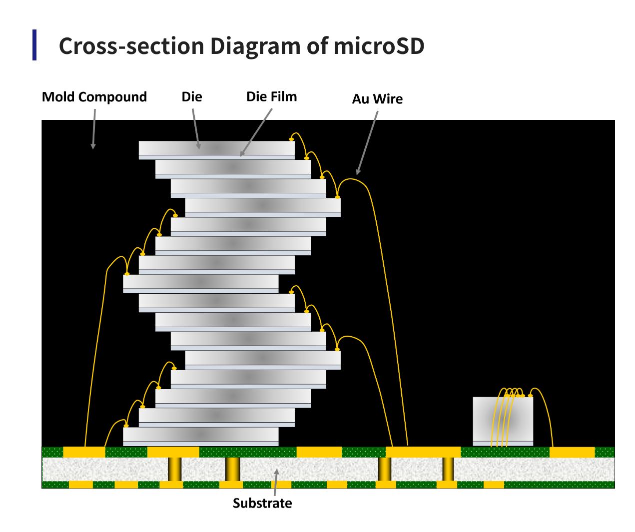
today I learned that we (as a civilization) now can put 16 silicon flash dice into a single 700µm microSD card on a commercial scale https://www.ose.com.tw/en/ic-services/memory-product-package/microsdsd
-
today I learned that we (as a civilization) now can put 16 silicon flash dice into a single 700µm microSD card on a commercial scale https://www.ose.com.tw/en/ic-services/memory-product-package/microsdsd
@whitequark @joe foolish rocks, you will do our microscopic bidding!
-
today I learned that we (as a civilization) now can put 16 silicon flash dice into a single 700µm microSD card on a commercial scale https://www.ose.com.tw/en/ic-services/memory-product-package/microsdsd
@whitequark Is this "3D NAND" and similar? I always wondered how they achieved the stacking!
-
if you think that the precariously balanced tower of flash above is an inaccurate representation of what's going on, i can reassure you that
(a) this is exactly how it looks like, and
(b) SK Hynix is up to 24 layers already (not sure in what application)
Semiconductor Back-end Process 4: Packages, Part 2
This article will explore packaging technologies that combine multiple packages and components within a single product.

SK hynix Newsroom - (news.skhynix.com)
@whitequark also each flash die has several hundred layers of stacked bit cells
-
@whitequark also each flash die has several hundred layers of stacked bit cells
@azonenberg yep! Samsung got up to 400 layers last year
-
@whitequark Is this "3D NAND" and similar? I always wondered how they achieved the stacking!
@attie no, 3D NAND is having (up to 400 in recent flash) layers of NAND cells in each die
-
@azonenberg yep! Samsung got up to 400 layers last year
@whitequark the last one i threw in the fib was "only" 176 iirc
-
today I learned that we (as a civilization) now can put 16 silicon flash dice into a single 700µm microSD card on a commercial scale https://www.ose.com.tw/en/ic-services/memory-product-package/microsdsd
@whitequark also looking at that diagram it seems like the 16 die stack is actually two 8 die onfi channels on top of each other mirrored with one coming out the left and one out the right
-
today I learned that we (as a civilization) now can put 16 silicon flash dice into a single 700µm microSD card on a commercial scale https://www.ose.com.tw/en/ic-services/memory-product-package/microsdsd
@whitequark now if we'd only build flash for a purpose other than storing content that's been stolen by our AI overlords
-
@attie no, 3D NAND is having (up to 400 in recent flash) layers of NAND cells in each die
@whitequark Oh, intriguing - thanks!
-
@azonenberg yep! Samsung got up to 400 layers last year
@whitequark @azonenberg No fucking way, how are those even economical to manufacture?

-
@whitequark @azonenberg No fucking way, how are those even economical to manufacture?
@0xC01DC0FFEE @whitequark V-NAND is crazy. Basically deposit alternating layers of a couple of materials then drill through the whole stack and you get a vertical abacus-shaped string of hundreds of flash bits
-
@0xC01DC0FFEE @whitequark V-NAND is crazy. Basically deposit alternating layers of a couple of materials then drill through the whole stack and you get a vertical abacus-shaped string of hundreds of flash bits
-
@whitequark @0xC01DC0FFEE the transistor channel is vertical polysilicon deposited into a hole that looks kinda like a dram capacitor, except it's ringed by ONO charge trap layers then more poly for the wordlines IIRC
-
R relay@relay.infosec.exchange shared this topic