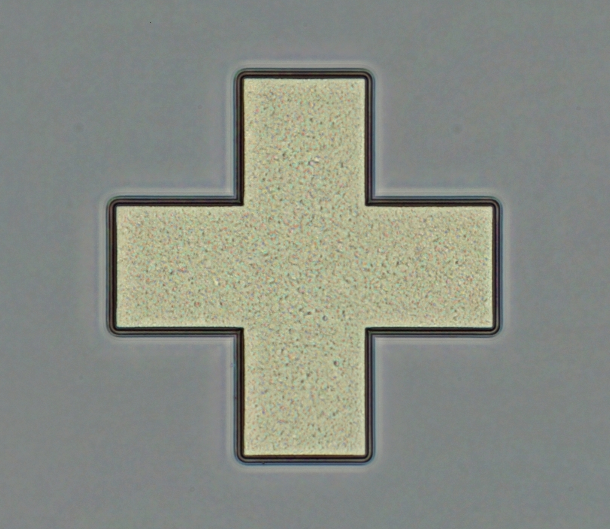
Hello and welcome to #NakedDieFriday!
-
Hello and welcome to #NakedDieFriday! This time with proper capitalisation.

The die of today is named HD6483153 and is designed by Hitachi. It fell out of a SIM card. I do not know what commercial p/n this is, if it was ever assigned one. If anyone can provide any details on what smart cards were made by Hitachi, please do so! In the meantime, we shall explore a bit. 🧵
Full-res map: http://infosecdj.net/map/hitachi/hd6483153/infosecdj_mz_nikpa40x_2/
#electronics #reverseengineering #smartcards
-
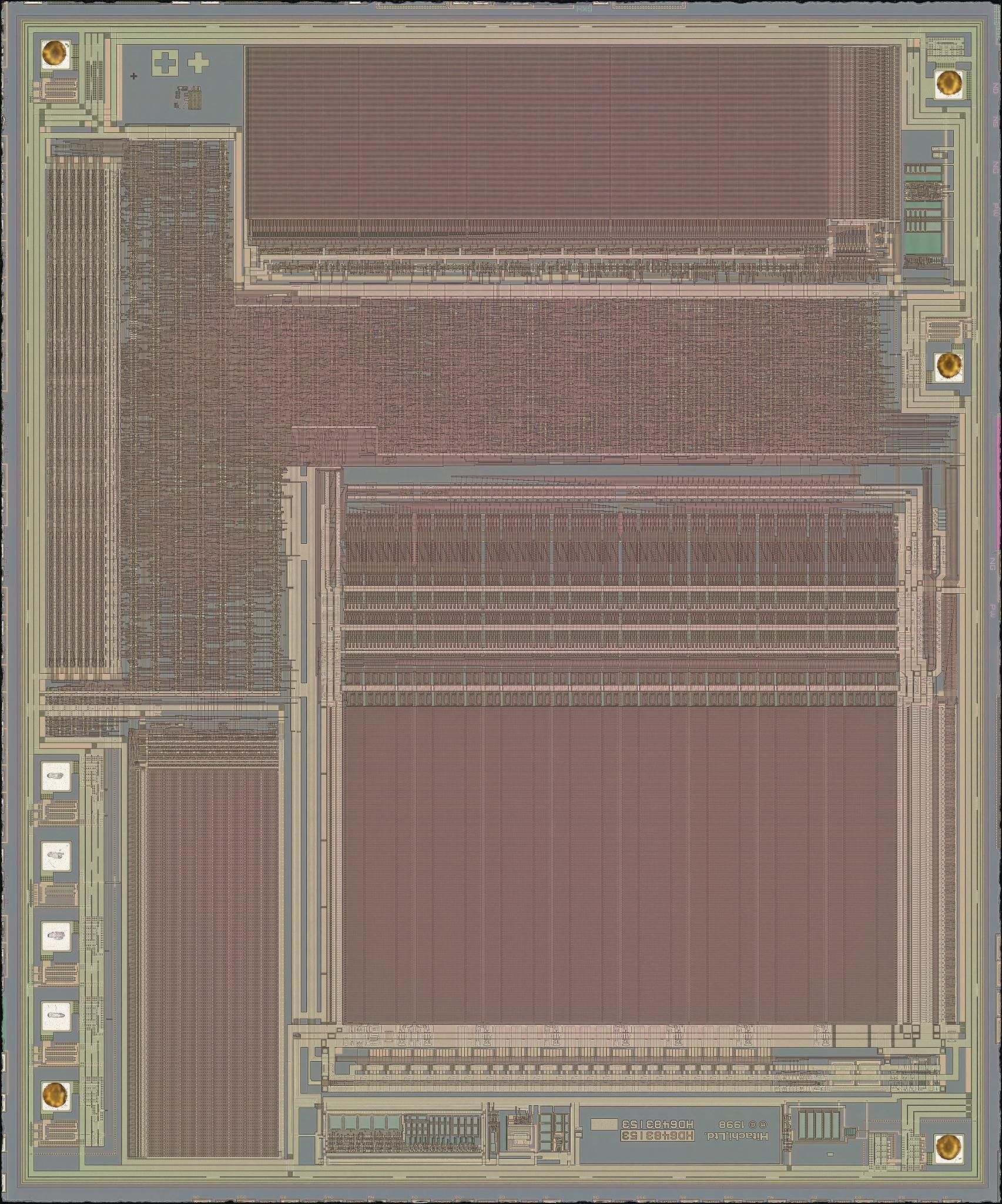
Hello and welcome to #NakedDieFriday! This time with proper capitalisation.
The die of today is named HD6483153 and is designed by Hitachi. It fell out of a SIM card. I do not know what commercial p/n this is, if it was ever assigned one. If anyone can provide any details on what smart cards were made by Hitachi, please do so! In the meantime, we shall explore a bit. 🧵
Full-res map: http://infosecdj.net/map/hitachi/hd6483153/infosecdj_mz_nikpa40x_2/
#electronics #reverseengineering #smartcards
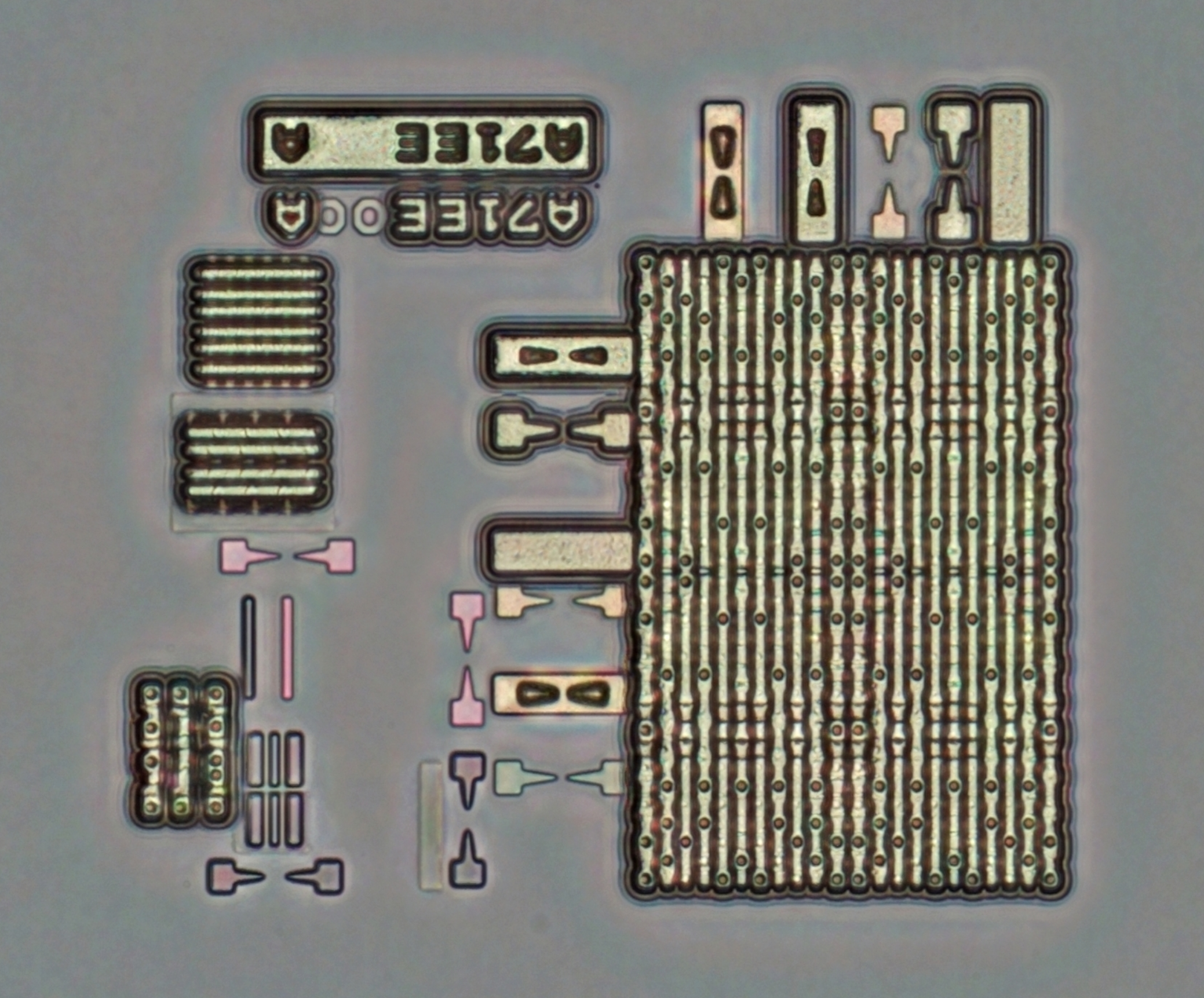
The die is fabbed using a 2-metal-layer CMOS process. The tightest routing on metal 1 seems to have 2u pitch. This can also be confirmed using these circuitry pieces. More or less.
Mask set IDs of some sort are there as well as alignment markings. Horizontal and vertical markings are separate.
-
The die is fabbed using a 2-metal-layer CMOS process. The tightest routing on metal 1 seems to have 2u pitch. This can also be confirmed using these circuitry pieces. More or less.
Mask set IDs of some sort are there as well as alignment markings. Horizontal and vertical markings are separate.
-
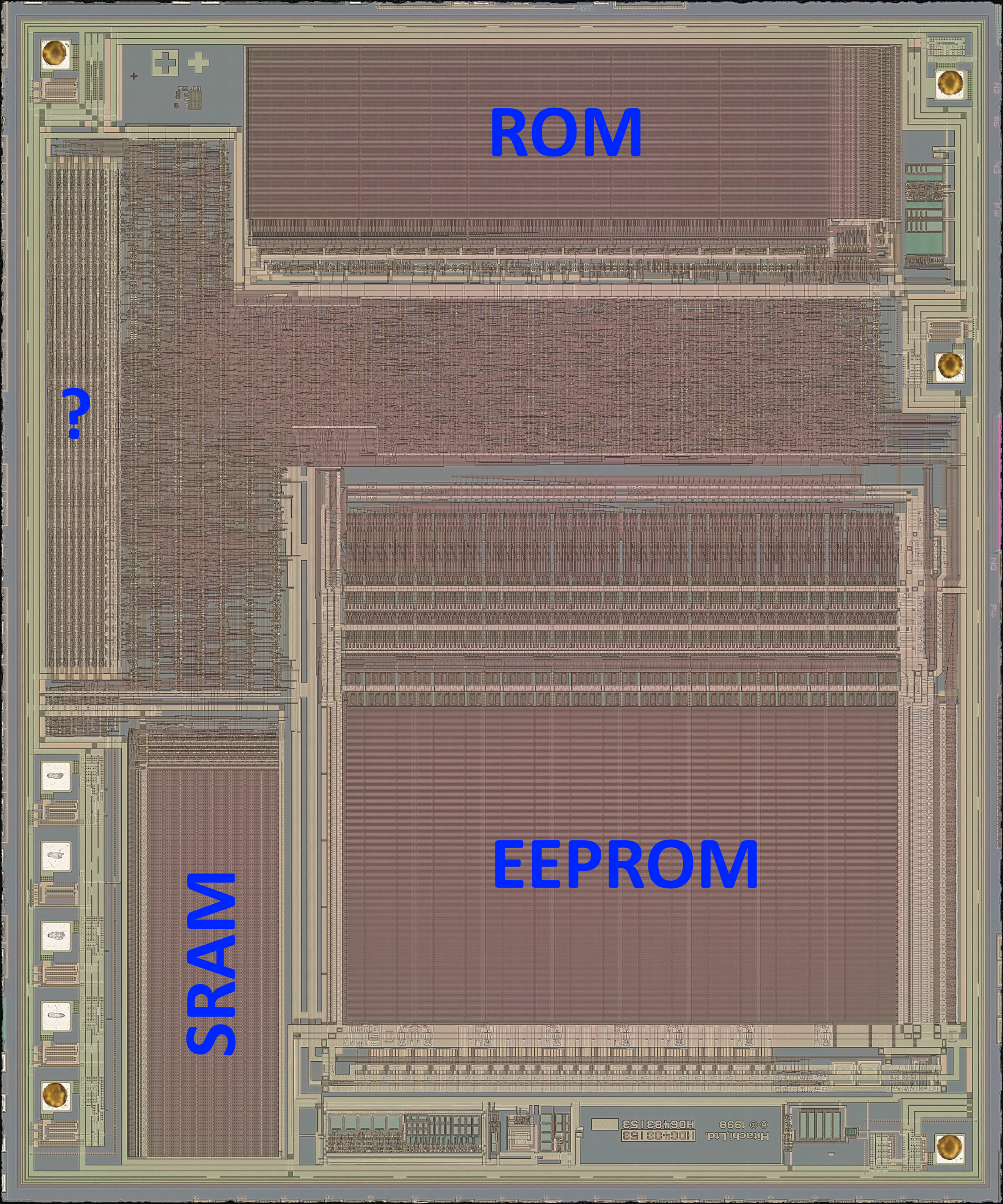
The design has everything one might expect a smartcard to have:
- A ROM unit in the upper part,
- A sea-of-gates implementing most of the logic right below it,
- An EEPROM taking more than 1/4 of the area,
- Some SRAM in the lower left.A unit marked with a question mark is of particular interest, as it has a very regular structure. This could be the CPU data path.
-
The design has everything one might expect a smartcard to have:
- A ROM unit in the upper part,
- A sea-of-gates implementing most of the logic right below it,
- An EEPROM taking more than 1/4 of the area,
- Some SRAM in the lower left.A unit marked with a question mark is of particular interest, as it has a very regular structure. This could be the CPU data path.
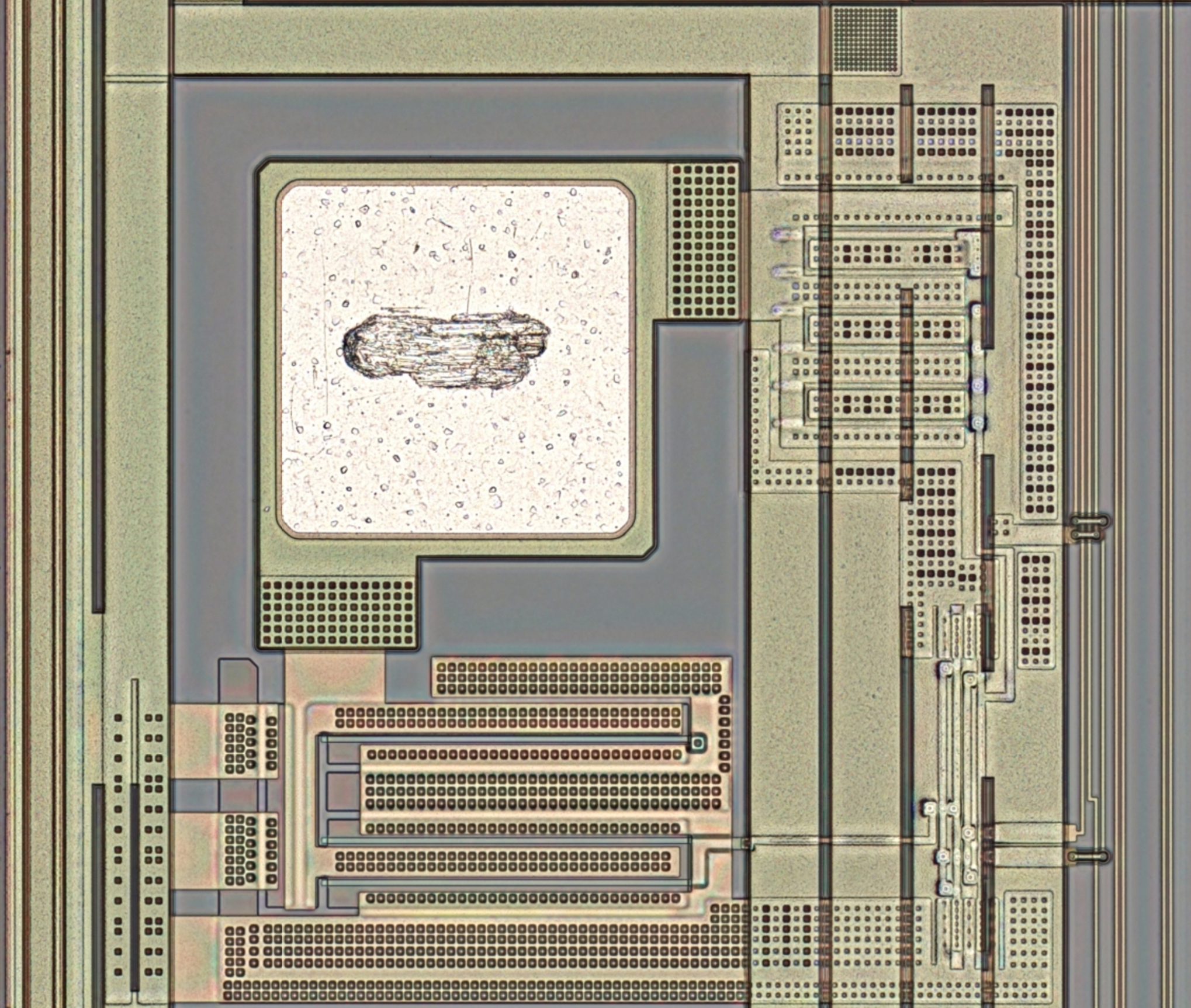
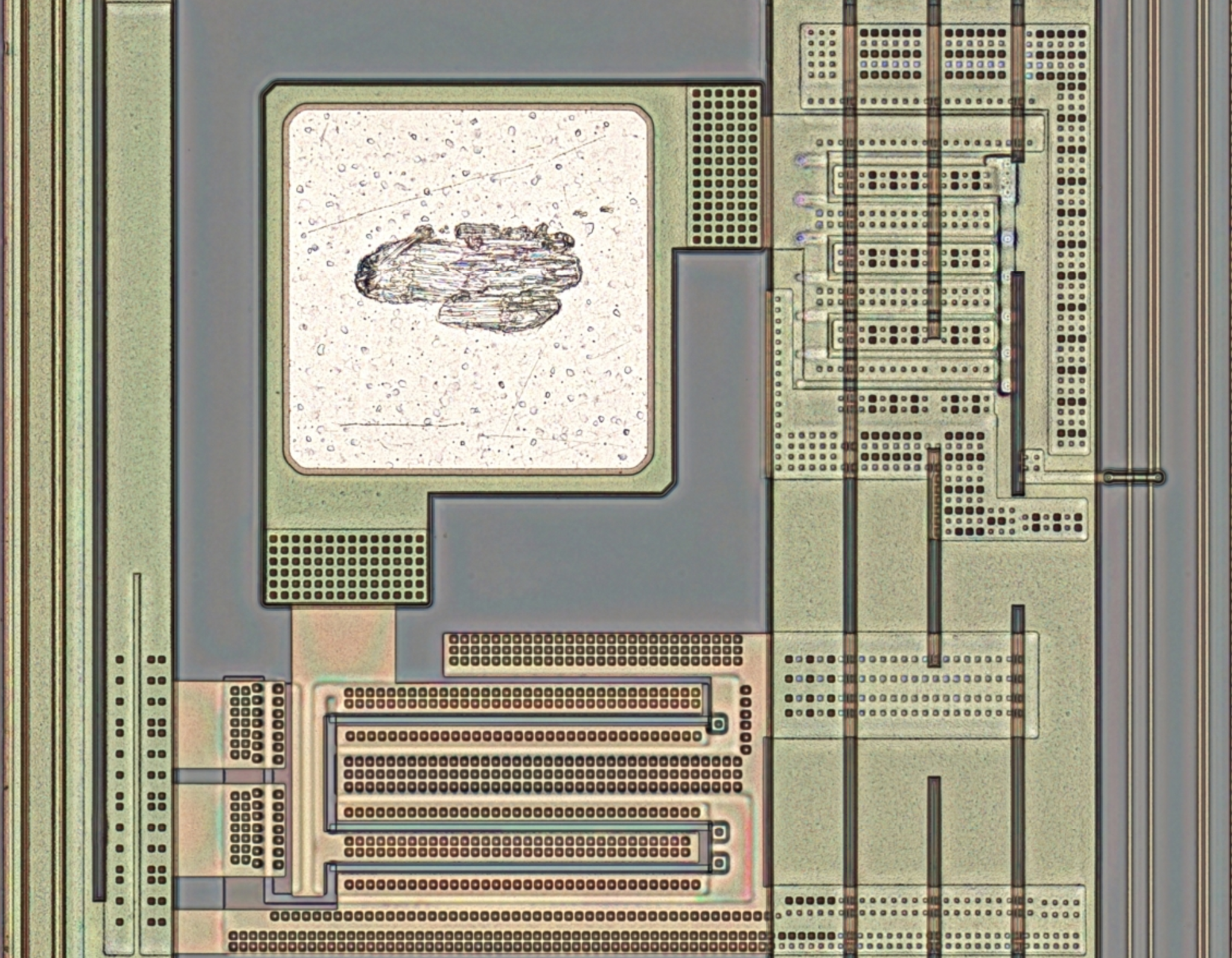
Apart from the usual set of 5 pads (VDD, VSS, RST, CLK, I/O), we have four more pads probed but not bonded. One is bidirectional, two are unidirectional and likely inputs, and one seems to be purely analog. The I/O pad has exactly the same structure as the bidirectional one.
-
Apart from the usual set of 5 pads (VDD, VSS, RST, CLK, I/O), we have four more pads probed but not bonded. One is bidirectional, two are unidirectional and likely inputs, and one seems to be purely analog. The I/O pad has exactly the same structure as the bidirectional one.
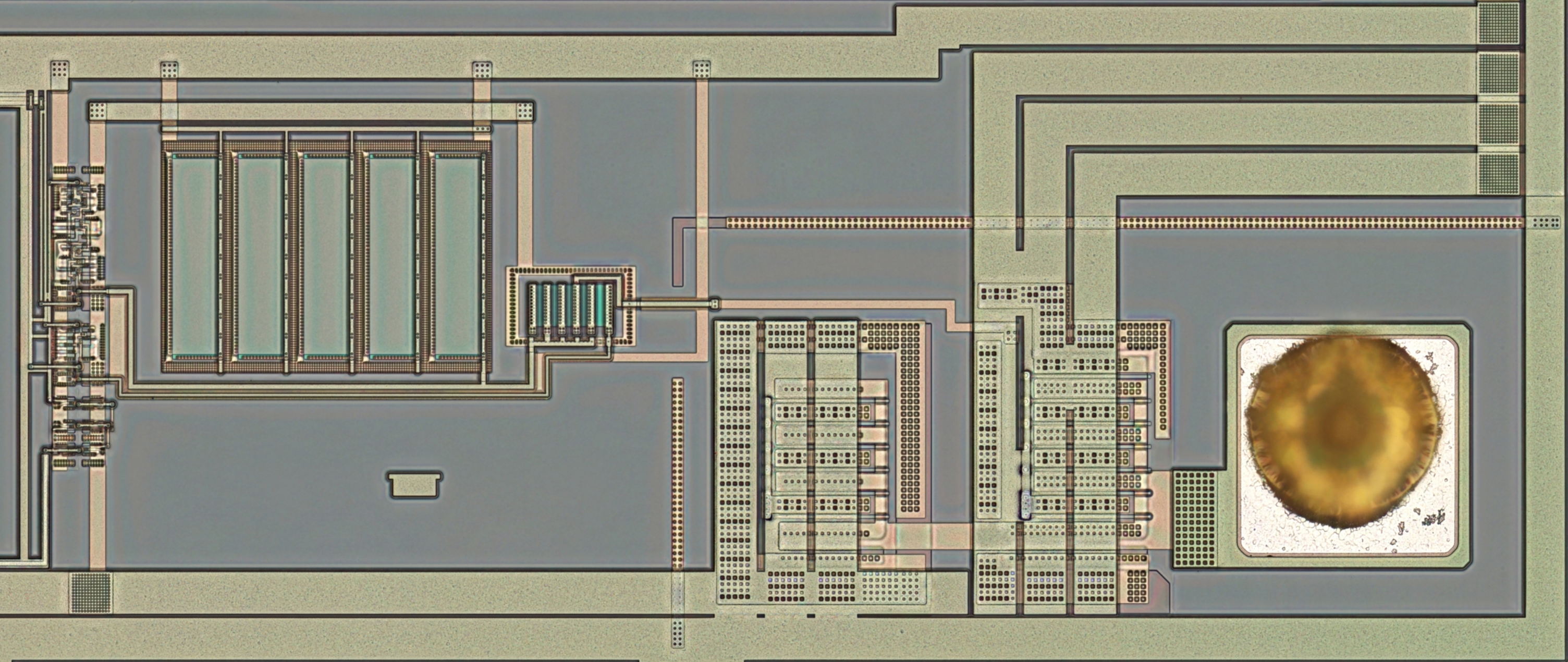
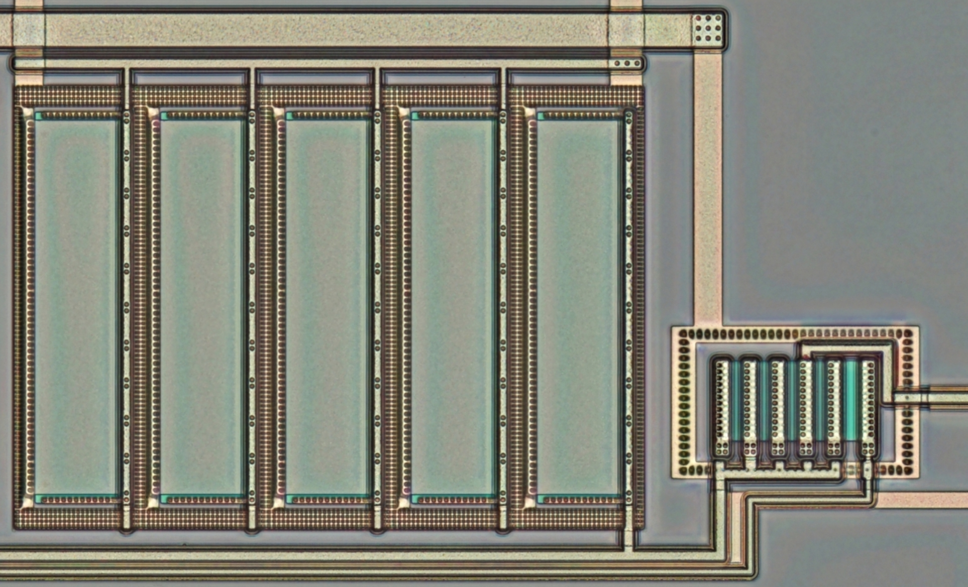
Unlike all the others, the clock input undergoes more conditioning. After ESD protection, it is filtered and further processed to produce four signals. These are then routed into more circuitry but it is hard to immediately say whether there is more filtering or they just use the received clock for something else.
The input filter seems to be a RC one with mask-selectable options for resistance and capacitance.
-
R relay@relay.infosec.exchange shared this topic