Years ago I had a "ReworkCTF" board with 20-odd PCB layout bugs designed into it on purpose, ranging from backwards LEDs to missing vias under a BGA to inner layer differential pair swaps.
-
@jpm this is specifically a rework/repair technician challenge not a debug challenge (although that might also be fun, it's a separate skill).
All of the defects will be well understood and documented. Your job is to apply the necessary ECO to make the board work as expected.
-
@jpm this is specifically a rework/repair technician challenge not a debug challenge (although that might also be fun, it's a separate skill).
All of the defects will be well understood and documented. Your job is to apply the necessary ECO to make the board work as expected.
@jpm so something like "missing pullup" is fine but the backstory of what the signal does is irrelevant. For the challenge it'd just be a weak on die pulldown configured on a GPIO that declares pass once it goes high.
-
Years ago I had a "ReworkCTF" board with 20-odd PCB layout bugs designed into it on purpose, ranging from backwards LEDs to missing vias under a BGA to inner layer differential pair swaps.
The original board had some design issues that made some of the fixes easier/harder than intended, and also ancient, I think now EOL, parts (a Spartan-3A FPGA - even if not EOL nobody wants to use one of those in 2026).
I'm hoping to do a gen 2 of the challenge soon probably based on a BGA STM32 or Spartan-7 but haven't worked out the specifics yet.
Is anybody interested in contributing challenge concept based on real board bugs you've had?
Also, would folks be interested in me livestreaming a "play through" of some/all of the challenges once I have a board in hand?
@azonenberg errata on this board so far:
- picked the wrong mid-mount USB-C port footprint and the pins just barely didn't reach the pads (USB2, so I just bodged a cut-up USB A cable onto it)
- assigned something to a gpio pin that wasn't suitable for it (needed PWM, picked a pin that couldn't do PWM)
- diode footprint slightly too short for diodes
others from past projects:
- picked the wrong width of SOIC footprint in both directions (IME, extending it outward with a bunch of parallel wires is easier than extending it inward, but both are entirely possible)
- all possible variations of "3-pin transistor or voltage regulator with the pins not in the order I thought they were"
- mirrored an asymmetric through-hole footprint (the style of barrel jack where one of the pins is on the side)
- the first board I ever sent off to a factory, I did not know what I was doing and somehow I sent an extra copy of my copper gerbers as my soldermask. they did not question it and happily sent me a board with soldermask perfectly applied only over the areas with no copper -
@jpm @ThermiteBeGiants Oh the swapped diffpair is gonna be 0.125mm which is min feature size for oshpark. Not much of a challenge if it's big
-
Years ago I had a "ReworkCTF" board with 20-odd PCB layout bugs designed into it on purpose, ranging from backwards LEDs to missing vias under a BGA to inner layer differential pair swaps.
The original board had some design issues that made some of the fixes easier/harder than intended, and also ancient, I think now EOL, parts (a Spartan-3A FPGA - even if not EOL nobody wants to use one of those in 2026).
I'm hoping to do a gen 2 of the challenge soon probably based on a BGA STM32 or Spartan-7 but haven't worked out the specifics yet.
Is anybody interested in contributing challenge concept based on real board bugs you've had?
Also, would folks be interested in me livestreaming a "play through" of some/all of the challenges once I have a board in hand?
@azonenberg
Tied an (unused) FPGA bank VCCO to ground and it really wanted go to a power on this device. 0.8mm bga two vcco pins per bank. Found an alternative workaround with no mods in real life, but I think I was showing our techs on of your blog posts at one point.Two ldos, one got copied from the other in schematic, and the vset and ilim net labels didn't get renamed. Just needed some surface cuts to split the nets.
-
Years ago I had a "ReworkCTF" board with 20-odd PCB layout bugs designed into it on purpose, ranging from backwards LEDs to missing vias under a BGA to inner layer differential pair swaps.
The original board had some design issues that made some of the fixes easier/harder than intended, and also ancient, I think now EOL, parts (a Spartan-3A FPGA - even if not EOL nobody wants to use one of those in 2026).
I'm hoping to do a gen 2 of the challenge soon probably based on a BGA STM32 or Spartan-7 but haven't worked out the specifics yet.
Is anybody interested in contributing challenge concept based on real board bugs you've had?
Also, would folks be interested in me livestreaming a "play through" of some/all of the challenges once I have a board in hand?
-
-
@azonenberg @jpm yeah looks to be, more boards for challenges with documented test stages would be great.
The smd soldering kits from china are helpful for learning, but they don't have any mid steps. It either works or doesn't and that isn't the best for figuring out what you did wrong. -
Years ago I had a "ReworkCTF" board with 20-odd PCB layout bugs designed into it on purpose, ranging from backwards LEDs to missing vias under a BGA to inner layer differential pair swaps.
The original board had some design issues that made some of the fixes easier/harder than intended, and also ancient, I think now EOL, parts (a Spartan-3A FPGA - even if not EOL nobody wants to use one of those in 2026).
I'm hoping to do a gen 2 of the challenge soon probably based on a BGA STM32 or Spartan-7 but haven't worked out the specifics yet.
Is anybody interested in contributing challenge concept based on real board bugs you've had?
Also, would folks be interested in me livestreaming a "play through" of some/all of the challenges once I have a board in hand?
@azonenberg - IC footprint with the pins in reverse order on one side
- depending on which pins in a (molex, etc) connector make contact first, an alternate path to ground exists through data lines that can't handle it -
@azonenberg @jpm yeah looks to be, more boards for challenges with documented test stages would be great.
The smd soldering kits from china are helpful for learning, but they don't have any mid steps. It either works or doesn't and that isn't the best for figuring out what you did wrong.@tj @jpm @azonenberg exactly. The main idea was to make a challenge board that is not super frustrating for beginners. And has lower requirements regarding tools and materials.
https://gitlab.aachen.ccc.de/cpresser/reworkctf-pico/-/blob/main/docs/Challenges.md?ref_type=headsThis was after I solved Andrews version and was not to happy with my own results
")
I am considering to make more of them (they are "sold out"), but have not yet decided if I want to add more challenges or edit challenges.
-
@tj @jpm @azonenberg exactly. The main idea was to make a challenge board that is not super frustrating for beginners. And has lower requirements regarding tools and materials.
https://gitlab.aachen.ccc.de/cpresser/reworkctf-pico/-/blob/main/docs/Challenges.md?ref_type=headsThis was after I solved Andrews version and was not to happy with my own results
I am considering to make more of them (they are "sold out"), but have not yet decided if I want to add more challenges or edit challenges.
@cccpresser @tj @jpm well I'm planning to do a rev2 in the next month or so, then livestream a playthrough
-
Years ago I had a "ReworkCTF" board with 20-odd PCB layout bugs designed into it on purpose, ranging from backwards LEDs to missing vias under a BGA to inner layer differential pair swaps.
The original board had some design issues that made some of the fixes easier/harder than intended, and also ancient, I think now EOL, parts (a Spartan-3A FPGA - even if not EOL nobody wants to use one of those in 2026).
I'm hoping to do a gen 2 of the challenge soon probably based on a BGA STM32 or Spartan-7 but haven't worked out the specifics yet.
Is anybody interested in contributing challenge concept based on real board bugs you've had?
Also, would folks be interested in me livestreaming a "play through" of some/all of the challenges once I have a board in hand?
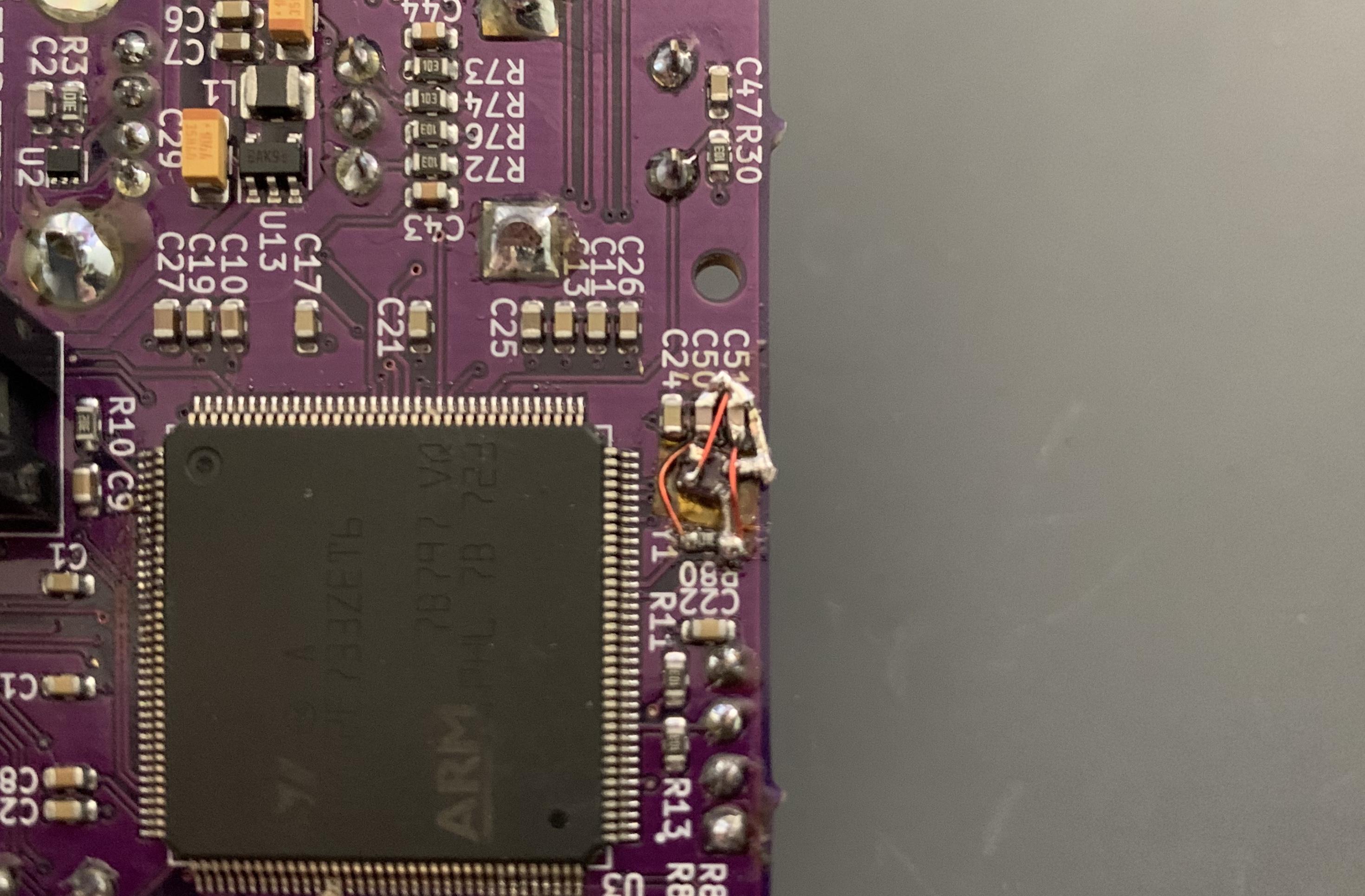
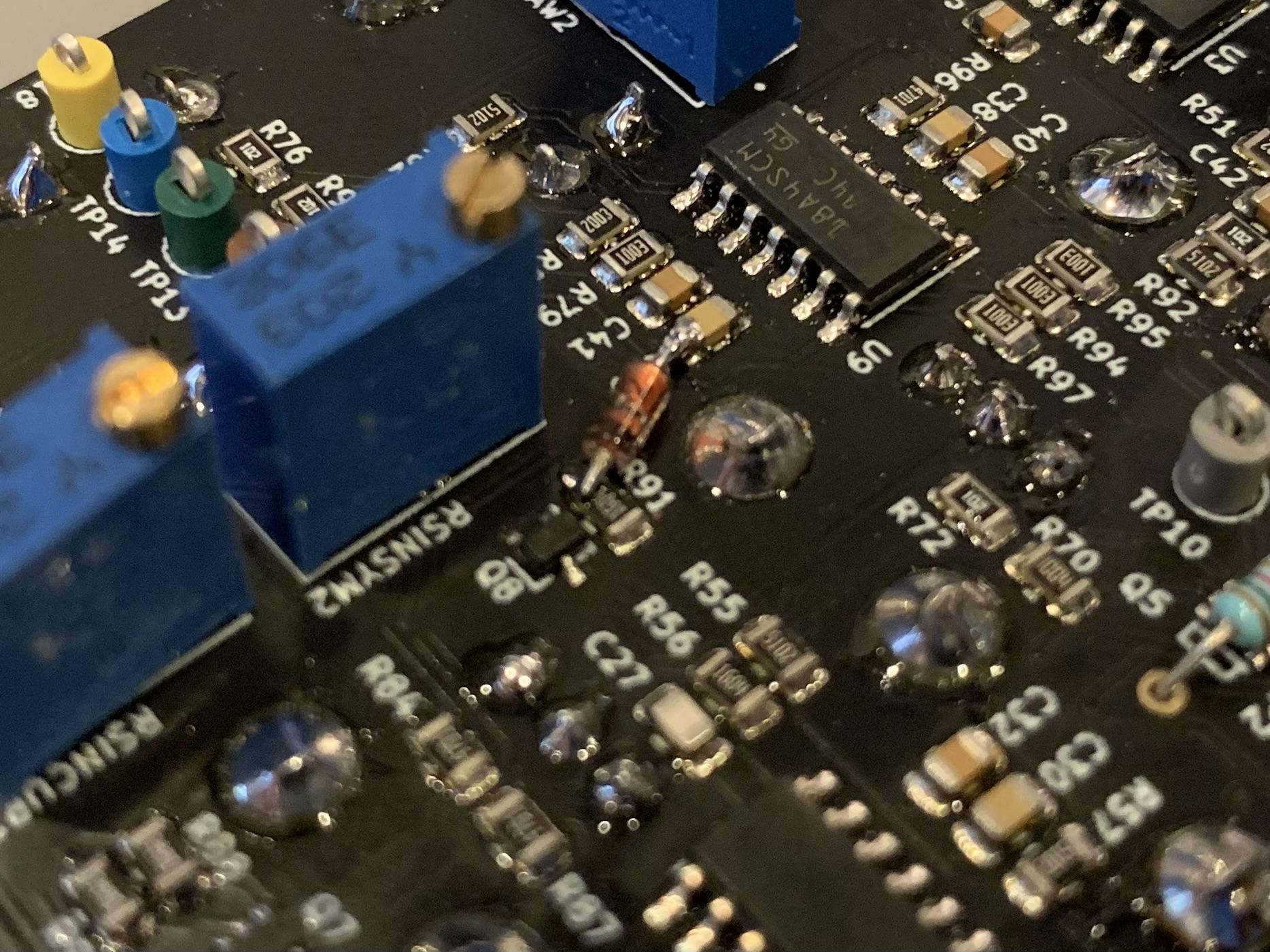
@azonenberg I thought I had more bodge pics, but here are a couple real ones
1st pic is wrong crystal footprint would be good. On this board I swapped the two gnd pads with the out and vcc pads. On a non-symmetric footprint too.
2nd pic is a bodged missing protection diode on a SOT transistor
-
@azonenberg I thought I had more bodge pics, but here are a couple real ones
1st pic is wrong crystal footprint would be good. On this board I swapped the two gnd pads with the out and vcc pads. On a non-symmetric footprint too.
2nd pic is a bodged missing protection diode on a SOT transistor
@azonenberg students can use my crystal bodge as an example of low quality rework

-
@cccpresser @tj @jpm well I'm planning to do a rev2 in the next month or so, then livestream a playthrough
@azonenberg @tj @jpm in that case, I will wait to see your rev2 and copy the new challenges and ideas that fit the "accessible" format as well.
My rough goal is to have a new version of my variant available for emfcamp.
-
@azonenberg students can use my crystal bodge as an example of low quality rework
-
R relay@relay.infosec.exchange shared this topic