I finally found a use for 32 layer PCBs!
-
I finally found a use for 32 layer PCBs!
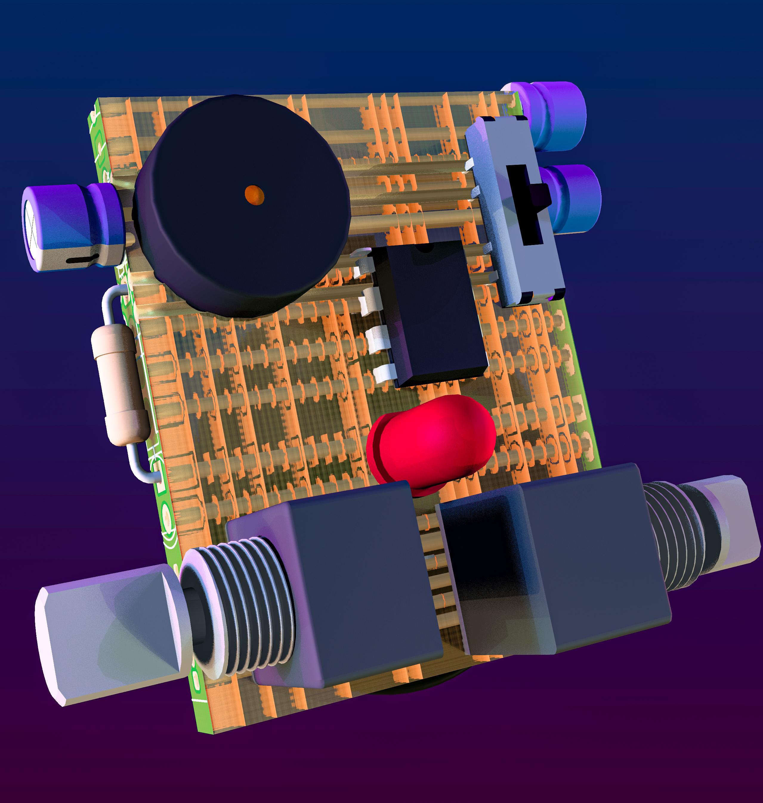
This is my worst and favorite idea I've had in a while.
-
I finally found a use for 32 layer PCBs!
@ArchiteuthisFlux what are you cooking up now?
-
I finally found a use for 32 layer PCBs!
@ArchiteuthisFlux this is beautifully cursed
-
I finally found a use for 32 layer PCBs!
-
@ArchiteuthisFlux what are you cooking up now?
@MLE_online Shitposts (but now I kinda want to make a real sideways PCB)
-
@MLE_online Shitposts (but now I kinda want to make a real sideways PCB)
@ArchiteuthisFlux i saw it and i believed this is something you would really do
-
I finally found a use for 32 layer PCBs!
@ArchiteuthisFlux this is horrible. Love it!
-
@ArchiteuthisFlux i saw it and i believed this is something you would really do
@MLE_online I just need like 1000 people to want these to amortize the insane $1200 "engineering fee."
I wonder if I could talk to a fab and let them know that this isn't some crazy radar board and they can do it kinda shitty.

-
I finally found a use for 32 layer PCBs!
@ArchiteuthisFlux
Cool, cool. How does this work on the wave solder machine, again? -
This is my worst and favorite idea I've had in a while.
It could also be fun to make this a solid cube of PCB with parts on all 6 sides
-
@ArchiteuthisFlux
Cool, cool. How does this work on the wave solder machine, again?@YetAnotherGeekGuy Just have them dunk the whole thing in solder
-
I finally found a use for 32 layer PCBs!
@ArchiteuthisFlux
Kevin.How long did it take you to multiply an entire circuit board’s locations by -1
-
@ArchiteuthisFlux
Kevin.How long did it take you to multiply an entire circuit board’s locations by -1
@JoshuaACNewman Way too long, but I was giggling to myself the whole time so it was worth it.
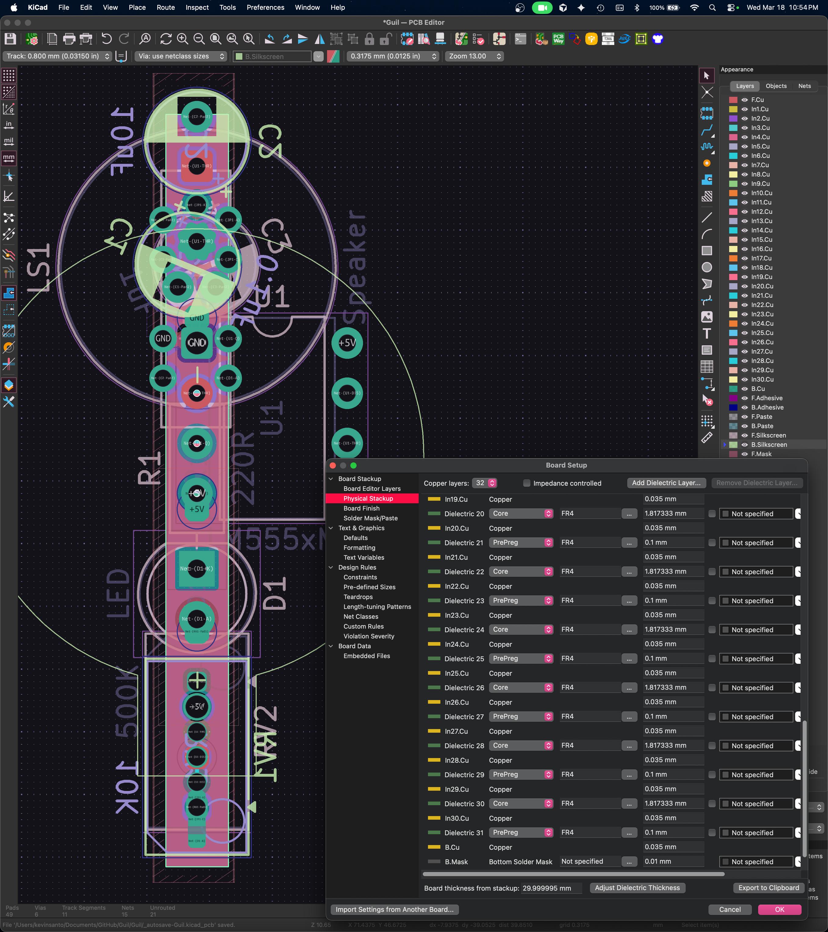
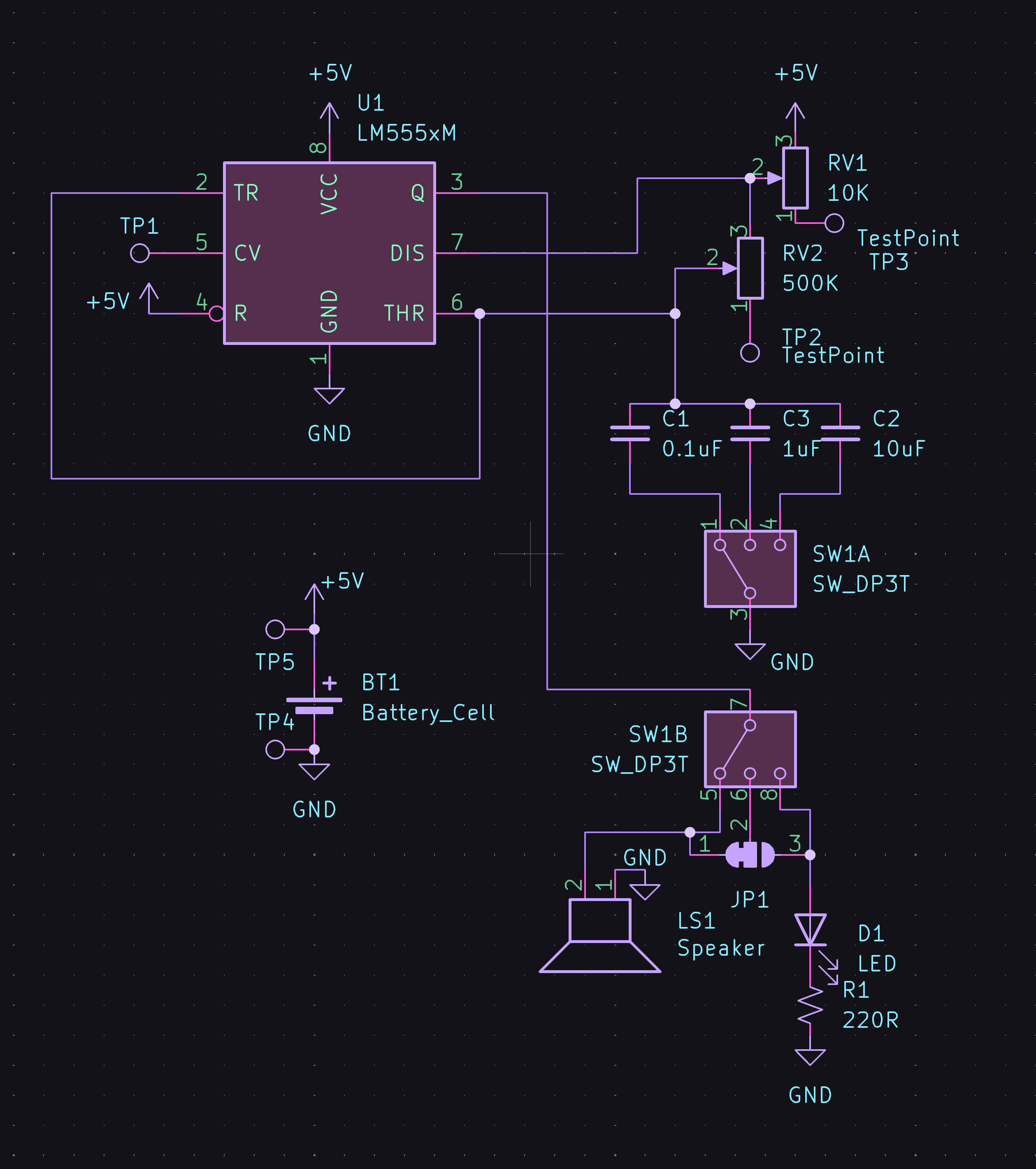
But the routing was weirdly easy, the vias already touch every layer so you just assign each fill a net and it connects them.
-
@JoshuaACNewman Way too long, but I was giggling to myself the whole time so it was worth it.
But the routing was weirdly easy, the vias already touch every layer so you just assign each fill a net and it connects them.
@ArchiteuthisFlux
Can you embed components within the layers? -
@ArchiteuthisFlux
Can you embed components within the layers?@JoshuaACNewman Yeah that's actually a thing. I haven't had the opportunity to use it, and I don't think I'd want to find myself in that situation.

Advanced: Embedded PCB Components - The Tech Blog
Based on a Reddit question, I thought I should address the topic of Embedded components on PCBs. In its simplest form, embedding components is the process of taking any parts like capacitors, resistors, or active ICs which you might place on the top and bottom layers to the inner layers of your PCB. This means […]
The Tech Blog (amaldev.blog)
-
@JoshuaACNewman Yeah that's actually a thing. I haven't had the opportunity to use it, and I don't think I'd want to find myself in that situation.
Advanced: Embedded PCB Components - The Tech Blog
Based on a Reddit question, I thought I should address the topic of Embedded components on PCBs. In its simplest form, embedding components is the process of taking any parts like capacitors, resistors, or active ICs which you might place on the top and bottom layers to the inner layers of your PCB. This means […]
The Tech Blog (amaldev.blog)
@ArchiteuthisFlux
Yeah, I know it’s a thing, I’m just daring you to double down. -
@MLE_online I just need like 1000 people to want these to amortize the insane $1200 "engineering fee."
I wonder if I could talk to a fab and let them know that this isn't some crazy radar board and they can do it kinda shitty.@ArchiteuthisFlux That's amazing! I'd chip in $10 to get a few of those boards.
-
I finally found a use for 32 layer PCBs!
@ArchiteuthisFlux cordwood 2.0
-
I finally found a use for 32 layer PCBs!
@ArchiteuthisFlux what have I just perceived
-
@ArchiteuthisFlux what have I just perceived
@Fishrock I love that this generates as much revulsion as my goatse footprint